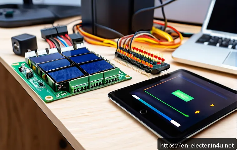
Electronics engineering and semiconductor engineering are closely connected, but they work at different layers of a product. Semiconductor specialists create or customize the chip, while electronics engineers integrate chips into boards, power systems, firmware, tests, and finished devices.
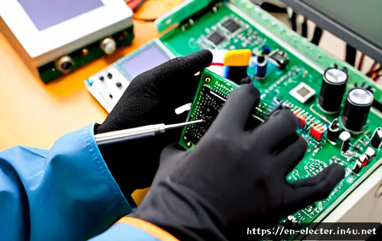
For many projects, strong electronics knowledge and standard components are enough; custom silicon becomes relevant when the product requires chip-level control or a specialized architecture.
The practical decision is not simply “build or buy,” but which skills, design automation tools, lab equipment, and engineering services match the project’s risk and scale.
Verification, packaging, thermal behavior, and production testing deserve attention as early as circuit selection. This guide compares the roles, workflows, and purchasing decisions behind semiconductor-enabled products.
At a Glance
- Semiconductors provide controllable electronic behavior for transistors, diodes, sensors, and integrated circuits.
- Electronic engineering turns semiconductor components into usable boards, embedded systems, power designs, and tested products.
- The right investment depends on whether the work is at the chip level, the board and system level, or both.
| Decision Area | Chip Design | PCB and System Design | Testing and Manufacturing Support |
|---|---|---|---|
| Main focus | Integrated circuit architecture, circuits, verification, and physical design | Component selection, board layout, power delivery, firmware, and integration | Validation, test methods, packaging considerations, reliability, and production readiness |
| Typical output | A chip design prepared for fabrication | A working electronic product or subsystem | Evidence that the product can be tested, assembled, and supported through production |
| Key tools | EDA software for simulation, verification, and physical design | PCB design, circuit simulation, embedded development, and documentation tools | Lab equipment, test fixtures, measurement workflows, and manufacturing documentation |
| Outsourcing fit | Often useful when internal chip-design specialization is limited | Useful for focused design, layout, firmware, or validation gaps | Useful when specialized test capability, packaging knowledge, or production support is needed |
The Short Answer: Why Chips and Electronic Systems Depend on Each Other
A semiconductor device is not a finished product on its own. It becomes useful when it is connected to power, signals, software, sensors, displays, communications hardware, or other system elements. This is why chip development and electronic engineering must work together from the earliest requirements stage.
Semiconductors provide the active devices inside modern electronics
Semiconductors are materials with electrical conductivity that can be controlled. That property makes them essential for transistors, diodes, sensors, and integrated circuits. An integrated circuit combines large numbers of electronic components on a semiconductor die, allowing a product to perform computing, sensing, control, signal handling, or power-related functions.
At this layer, engineering decisions concern device behavior, circuit operation, and the design of the integrated circuit itself. These choices influence what the rest of the product can do, but they do not remove the need for careful board, firmware, and test work.
Electronics engineering turns chips into useful products and systems
Electronic engineers commonly work with semiconductor components after, or alongside, chip development. Their scope can include circuit theory, signal analysis, power design, embedded systems, validation, and reliability testing. They decide how components interact on a board and how the full system behaves in real operating conditions.
For example, selecting a capable integrated circuit is only one part of a hardware decision. The board must deliver suitable power, route signals appropriately, support the required firmware, and provide a practical way to test the final device. A high-performing chip can still create product problems if the system around it is poorly designed or insufficiently validated.
Where the two disciplines overlap—and where they differ
The overlap is strongest around specifications, simulation, verification, test, thermal considerations, and reliability. Both disciplines use design automation tools to reduce uncertainty before production. The difference is mainly one of level: semiconductor engineering focuses on the chip and its manufacturing path, while electronics engineering usually focuses on the board, system, firmware, and final product behavior.
Do not treat the boundary as absolute. A chip package can affect board layout, electrical performance, heat flow, and reliability. Likewise, system requirements can force changes in chip architecture or component selection. Product teams need a clear handoff, but they also need active communication across both sides.
From Silicon to Product: The Engineering Chain
A semiconductor-enabled product moves through a connected engineering chain. The work commonly includes specification, architecture, circuit design, verification, physical design, fabrication, packaging, and testing. The board and system work must fit around that chain rather than begin after every chip decision is fixed.
Device physics, transistor behavior, and integrated circuit design
Chip-level work starts with a clear specification. Engineers translate the intended function into architecture, circuit design, verification plans, and physical design. The objective is not only to create a circuit that appears correct in concept, but to verify and document the design before production.
EDA software is central here because it supports simulation, verification, and design documentation. A team evaluating semiconductor design tools should first define what must be simulated or verified, who will use the tools, and how the output fits into the broader design flow. Buying a tool without a defined verification process can add expense without resolving project risk.
PCB design, power delivery, firmware, and system integration
At the electronics level, engineers select components and build the environment in which those components operate. This includes PCB design, signal paths, power delivery, embedded firmware, interfaces, and system-level validation. The goal is a product that does more than power on: it should behave consistently across its intended use conditions.
Power design and signal analysis are especially important because chips depend on stable electrical conditions. A design decision that looks minor on a schematic may affect performance when the device is assembled and tested. Early coordination between PCB designers, firmware developers, and semiconductor specialists helps expose these dependencies before production commitments are made.
Verification, test, packaging, and reliability across the lifecycle
Verification and testing are not final-step chores. They are part of the design strategy. Chip development uses verification before production, while electronic product development needs validation of the board, firmware, interfaces, and final system.
Packaging and thermal management also matter across the lifecycle. A package influences how a chip connects electrically and how heat moves through the finished product. Those factors can strongly affect electrical performance, reliability, and suitability for a real device. Teams should include packaging assumptions and thermal considerations in design reviews instead of treating them as manufacturing details.
Comparing Chip Design, Electronics Design, and Manufacturing Support
The best path depends on the product’s technical requirements and the skills already available. A company does not need to own every capability, but it does need to understand which capability is missing and how that gap affects verification, cost, and production readiness.
Skills, software, equipment, and project outputs
Chip design work may require semiconductor specialization, architecture knowledge, circuit design ability, verification discipline, and physical design expertise. Electronics design often requires board-level circuit knowledge, power and signal analysis, embedded systems work, and product testing skills. Manufacturing support adds another set of needs: controlled assembly, practical testing, packaging awareness, and reliability-focused processes.
Engineering software should match the work being done. An EDA tool for chip verification serves a different purpose from a PCB tool or embedded development environment. Similarly, lab equipment should support defined measurements and test plans, not merely fill a lab bench. Before purchasing, identify the required output: simulation evidence, design files, test data, firmware validation, or production documentation.
In-house development versus specialist engineering services
In-house development can make sense when the organization needs ongoing control of product knowledge and expects repeated use of the same capability. Specialist engineering services can be useful when a project needs a narrow skill set, such as semiconductor design, verification, PCB layout, thermal review, test-fixture development, or manufacturing preparation.
A practical question is: Can the internal team define, review, and validate the outside partner’s deliverables? If not, outsourcing may shift work but not reduce risk. A capable engineering consultancy or semiconductor design service should be evaluated by its process, documentation, handoff method, verification approach, and ability to work with the existing product team.
Cost and value factors beyond the initial prototype
A prototype is only one milestone. The complete value calculation should include verification, repeated testing, design documentation, packaging considerations, thermal management, test fixtures, and the ability to support production volume. These factors may matter more than the first version of the board or circuit.
Fabrication also requires specialized cleanroom facilities, process equipment, and tightly controlled materials. That is one reason custom semiconductor work is fundamentally different from selecting standard components for an electronics design. Exact fabrication costs, tool subscription prices, lead times, and service terms vary by project, provider, location, and market conditions, so they require direct confirmation.
Practical Workflow and Common Mistakes to Avoid
A reliable workflow starts with the system outcome, then works backward into component, board, firmware, test, and manufacturing decisions. This reduces the chance of optimizing one layer while creating a problem in another.

Start with system requirements before selecting a chip
Define the product function first. What signals must it handle? What power behavior, sensing, processing, connectivity, and firmware functions are required? Once these questions are clear, the team can decide whether an off-the-shelf semiconductor component is suitable or whether deeper chip-level work should be explored.
Avoid choosing a chip solely from a headline specification. Semiconductor specifications are important, but commercial success cannot be determined from chip specifications alone. The product also needs workable system integration, testing, manufacturing support, and a path to reliable operation.
Plan for signal integrity, thermal limits, power consumption, and compliance
Signal behavior, power delivery, and heat should be considered during architecture and board planning. These areas interact: electrical design affects thermal behavior, and packaging can affect both electrical performance and reliability. A system review should ask whether the selected package, board layout, power path, and test plan support the intended product use.
Where compliance requirements apply, confirm the relevant needs for the target product and market with appropriate technical and manufacturing stakeholders. Requirements differ by product category and destination, so they should not be assumed from another project.
Avoid underestimating validation, test fixtures, and supply-chain risk
Validation requires a plan, measurable conditions, and suitable test access. A board that is difficult to probe or a device that lacks a clear test method can slow engineering decisions later. Test fixtures, repeatable procedures, and well-documented results help teams compare revisions and prepare for manufacturing support.
Supply-chain questions also belong in the early review. Product teams should confirm component availability assumptions, approved alternatives where appropriate, and how a manufacturing partner will manage changes. This is not a reason to delay every decision; it is a reason to make dependencies visible before the design is difficult to change.
Which Path Fits Your Goal?
The appropriate learning or sourcing path differs for students, startups, and established businesses. The shared principle is simple: build or obtain the capabilities needed for the next decision, rather than pursuing every specialization at once.
Students building foundational skills for electronics or semiconductor roles
Students can begin with circuit theory, signal analysis, power concepts, embedded systems, and testing. These skills create a practical base for electronics roles and make semiconductor topics easier to understand. Those interested in chip development can then explore integrated circuit design, verification, physical design, and the use of chip-focused EDA software.
Build evidence of process, not only finished projects. Document requirements, simulations, design choices, test results, and revisions. This mirrors the way engineering teams communicate and helps distinguish a working demonstration from a repeatable engineering result.
Startups selecting off-the-shelf chips versus custom silicon
Startups should begin by asking whether standard semiconductor components can meet the system requirement. Using existing chips may allow the team to focus on PCB design, firmware, validation, packaging integration, and product testing. Custom semiconductor design introduces a broader chain of architecture, verification, physical design, fabrication, packaging, and testing.
A custom approach should be considered only after the product requirement is specific enough to justify chip-level specialization. The decision should account for the full engineering path, not simply the perceived advantage of owning a unique chip design.
Businesses evaluating design consultancies, contract manufacturers, or test partners
Businesses can divide the evaluation into three questions: What must be designed? What must be verified? What must be supported through manufacturing? A design consultancy may help with architecture, electronics design, firmware, or validation. A contract manufacturer may contribute manufacturing feedback. A test partner may help establish repeatable methods and production-oriented testing.
Request clarity on deliverables, documentation, verification responsibilities, testing boundaries, and handoff ownership. These points are more useful than broad claims of expertise because they show how the provider fits into the actual engineering chain.
Selection Criteria and Comparison Summary
Before selecting EDA software, lab equipment, or an engineering service provider, check the following:
- Project layer: Is the need chip architecture, PCB and system integration, firmware, testing, or manufacturing support?
- Verification need: What must be simulated, measured, reviewed, and documented before production?
- Internal ownership: Which decisions and deliverables can the internal team evaluate and maintain?
- Thermal and packaging fit: Have electrical performance, heat management, and reliability been reviewed together?
- Production path: Does the plan include test access, fixtures, documentation, and manufacturing feedback?
- Scalability: Can the design and support model adapt if the product requirements or production volume change?
When comparing engineering software subscriptions, test equipment, or design partners, review the official scope, technical requirements, support terms, and deliverables on the relevant provider page before making a commitment.
Closing Thoughts
Semiconductor engineering and electronics engineering are not competing paths. They are connected layers of the same product-development process. Chips provide the active functions, while electronic engineering makes those functions useful in a complete system. The strongest decisions begin with product requirements and include verification, testing, packaging, and manufacturing planning from the start.
Useful Things to Know
1. Integrated circuits place many electronic components on a semiconductor die.
2. Electronic engineers often work with semiconductor components at the board, system, firmware, validation, and reliability levels.
3. Design automation tools support simulation, verification, and documentation before production.
4. Packaging and thermal management can affect electrical performance, reliability, and final-product suitability.
Important Considerations
No single degree, EDA software package, lab setup, semiconductor vendor, or engineering partner is universally best. Tool pricing, fabrication costs, hiring conditions, project lead times, and available services vary by location, company, project complexity, and market conditions. Confirm technical scope, commercial terms, and production assumptions directly with the relevant provider before deciding.
Frequently Asked Questions
Q1. What is the main difference between semiconductor engineering and electronic engineering?
A1. Semiconductor engineering focuses more directly on the devices and integrated circuits built on semiconductor materials, including chip architecture, circuit design, verification, physical design, fabrication, packaging, and testing. Electronic engineering focuses on using those components in boards, power systems, embedded systems, and finished products. The disciplines overlap in areas such as simulation, testing, reliability, and system requirements.
Q2. When should a company use standard chips instead of paying for custom semiconductor design?
A2. Standard chips are worth considering when they meet the required system function and allow the team to concentrate on product integration, PCB design, firmware, validation, and manufacturing preparation. Custom semiconductor design may become relevant when product requirements demand chip-level specialization. Compare the full development chain, including verification, fabrication, packaging, and testing, rather than comparing only the initial design concept.
Q3. What tools and services should a startup compare before developing an electronic hardware product?
A3. Start with the tools needed for the actual work: circuit or PCB design, simulation, embedded development, documentation, and product testing. Then identify whether specialist services are needed for chip design, verification, board layout, thermal review, test fixtures, or manufacturing support. Compare each option by technical scope, expected deliverables, verification workflow, documentation quality, and how well it fits the startup’s internal engineering capability.