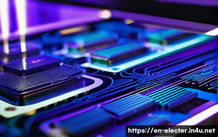
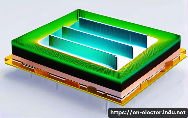
Understanding semiconductor process technology is essential in today’s tech-driven world, where tiny chips power everything from smartphones to electric cars.

This intricate field involves transforming raw materials into highly complex integrated circuits through precise manufacturing steps. Grasping these processes not only reveals how modern electronics function but also highlights the innovation behind faster, smaller, and more efficient devices.
Whether you’re a tech enthusiast or a professional, diving into semiconductor fabrication opens up a fascinating glimpse into the future of technology.
Let’s explore the details together and uncover what makes this industry tick!
Fundamental Steps in Semiconductor Fabrication
Wafer Preparation and Cleaning
The journey of making a semiconductor chip begins with the silicon wafer, a thin slice of highly purified silicon crystal. These wafers must be meticulously cleaned to remove any microscopic particles, organic residues, or metal contaminants that could jeopardize the delicate circuit patterns.
In my experience visiting fabrication plants, the cleaning process involves multiple stages using chemical baths like piranha solution and hydrofluoric acid, followed by ultra-pure water rinses.
This ensures an ultra-clean surface, critical for the next steps where even a speck of dust can ruin the entire chip. The precision and care taken here really highlight the complexity behind something that seems so simple.
Photolithography: Painting the Circuit
Photolithography is the artistic heart of semiconductor manufacturing. Think of it as projecting a detailed blueprint of the circuit onto the wafer’s surface using light and special photosensitive materials called photoresists.
The wafer is coated with this photoresist, then exposed to ultraviolet light through a mask that carries the circuit design. The exposed areas become soluble, allowing selective removal and revealing patterns down to the nanometer scale.
Walking through cleanrooms, I’ve seen how this step demands extreme accuracy—temperature, light intensity, and timing must be perfectly controlled. This process is repeated many times to build complex multilayered chips, each layer adding new functionality.
Etching and Deposition: Sculpting the Layers
Once the pattern is set, the wafer undergoes etching, where chemical or plasma processes remove unwanted silicon or other materials to create the physical structures of the circuit.
There are dry etching methods like reactive ion etching that allow for precise, anisotropic cuts and wet etching for more general material removal. After etching, deposition techniques add thin films of metals, insulators, or semiconductors—layer by layer—to build the transistor gates, interconnects, and insulating barriers.
Techniques like chemical vapor deposition (CVD) and physical vapor deposition (PVD) are common here. From personal observation, these steps are a dance of chemistry and physics, where every variable impacts the chip’s final performance.
Advanced Techniques Driving Moore’s Law Forward
Extreme Ultraviolet Lithography (EUV)
EUV lithography represents a breakthrough in shrinking transistor sizes beyond traditional limits. Unlike conventional photolithography that uses deep ultraviolet light, EUV employs much shorter wavelengths around 13.5 nm, allowing for finer patterning on the wafer.
I remember reading about the immense engineering feats behind EUV machines, including complex mirrors and vacuum systems, which make this technology expensive but indispensable for the latest chips powering smartphones and servers.
This innovation is what keeps Moore’s Law alive, enabling more transistors to fit on smaller chips with improved energy efficiency.
FinFET and 3D Transistor Structures
To combat leakage currents and boost performance at tiny scales, the industry transitioned from planar transistors to FinFET (fin field-effect transistor) designs.
Instead of flat surfaces, FinFETs use vertical fins that increase the channel control between source and drain. I’ve seen detailed SEM images showing how these fins rise like tiny skyscrapers on the silicon surface.
This 3D approach enhances switching speed and reduces power consumption, a key reason why modern processors are both faster and cooler compared to older generations.
Materials Beyond Silicon
While silicon remains the dominant semiconductor material, researchers and manufacturers are exploring alternatives like silicon carbide (SiC), gallium nitride (GaN), and even 2D materials such as graphene.
These materials offer superior electrical properties for specialized applications like power electronics and high-frequency devices. In conversations with engineers, it’s clear that material innovation is as crucial as lithography advances for future tech.
For instance, electric vehicles benefit greatly from SiC’s high-temperature tolerance and efficiency, driving the push toward greener transportation.
Quality Control and Testing in Semiconductor Manufacturing
Inline Metrology and Defect Inspection
Throughout fabrication, wafers undergo continuous inspection to catch defects early. Inline metrology tools measure layer thickness, critical dimensions, and surface roughness with nanometer precision.
Automated optical inspection systems scan for particles, pattern misalignments, or etching errors. From firsthand accounts of fab floor visits, these quality controls are vital since a single defect can cause chip failure, leading to costly recalls.
The integration of AI-powered image recognition has significantly enhanced defect detection speed and accuracy.
Electrical Testing and Yield Analysis
After fabrication, wafers proceed to electrical testing where each chip’s transistors and interconnects are probed to verify functionality. This process identifies faulty units before packaging.
Yield analysis then calculates the percentage of usable chips per wafer, guiding process improvements. I’ve learned that improving yield even by a fraction of a percent can translate to millions of dollars saved, highlighting the economic impact of stringent testing.
Burn-in and Reliability Stress Testing
To ensure chips can withstand real-world operating conditions, manufacturers perform burn-in tests that run devices at elevated temperatures and voltages.
This accelerates aging and reveals early-life failures. Reliability tests also simulate conditions like thermal cycling and electromigration stresses.

My discussions with reliability engineers revealed that this stage is crucial for products like automotive controllers where failure is not an option.
Key Semiconductor Process Technologies Compared
| Process Step | Description | Common Techniques | Impact on Chip Performance |
|---|---|---|---|
| Wafer Cleaning | Removing contaminants from the silicon surface | Chemical baths, megasonic cleaning | Prevents defects, ensures pattern fidelity |
| Photolithography | Patterning circuit designs onto wafers | UV lithography, EUV lithography | Defines transistor size and density |
| Etching | Removing material to form circuit features | Reactive ion etching, wet etching | Shapes transistor structures, affects electrical properties |
| Deposition | Adding thin films of materials | CVD, PVD, atomic layer deposition (ALD) | Builds functional layers like gates and interconnects |
| Testing | Verifying chip functionality and reliability | Electrical probing, burn-in tests | Ensures product quality and longevity |
Challenges and Innovations in Scaling Down
Overcoming Physical Limitations
Shrinking transistor sizes below 5 nanometers introduces quantum mechanical effects like tunneling, which can cause leakage currents and heat generation.
I’ve followed industry debates on how to mitigate these issues, with solutions ranging from novel transistor architectures to advanced materials. It’s fascinating how chipmakers balance physics constraints with manufacturing feasibility, pushing the boundaries of what’s possible.
Cost and Complexity of Fabrication Facilities
Building and operating a state-of-the-art semiconductor fab costs billions of dollars. The capital investment rises sharply with each new technology node due to equipment complexity, cleanroom standards, and process controls.
I recall reading that leading-edge fabs require over 10,000 process steps and employ thousands of people worldwide. This enormous scale drives consolidation in the industry, with only a few players able to afford cutting-edge production.
Environmental and Sustainability Considerations
The semiconductor industry consumes vast amounts of water, energy, and chemicals. Recent efforts focus on reducing environmental impact through water recycling, green chemistry, and energy-efficient equipment.
From environmental reports I’ve reviewed, companies increasingly prioritize sustainability, recognizing that future growth depends on balancing innovation with ecological responsibility.
The Role of Semiconductor Technology in Emerging Applications
AI and Machine Learning Hardware
Advanced semiconductor chips power AI workloads by providing massive parallel processing capabilities. Technologies like 3D stacking and specialized accelerators optimize data throughput and energy efficiency.
I’ve seen firsthand how these chips enable breakthroughs in natural language processing and computer vision, transforming industries from healthcare to autonomous driving.
5G and Communication Devices
The rollout of 5G networks demands chips capable of high-frequency operation with low latency. Semiconductor process advancements enable smaller, faster RF components and system-on-chip (SoC) designs that support complex communication protocols.
Industry insiders often highlight how these improvements directly impact user experience through faster downloads and more reliable connections.
Electric Vehicles and Power Electronics
Semiconductor innovations in power management chips improve the efficiency and range of electric vehicles. Wide-bandgap materials like SiC and GaN enable higher voltage operation and reduce energy losses.
Conversations with EV manufacturers underscore how these advances contribute to more affordable and sustainable transportation options.
글을 마치며
Semiconductor fabrication is a marvel of precision, innovation, and relentless pursuit of excellence. From wafer preparation to cutting-edge lithography and testing, each step shapes the technology that powers our digital world. Understanding these processes not only highlights the complexity behind everyday devices but also inspires appreciation for the engineers and scientists driving this ever-evolving industry forward.
알아두면 쓸모 있는 정보
1. The cleanliness of silicon wafers is absolutely critical; even the tiniest particle can cause defects that ruin entire batches of chips.
2. Photolithography involves multiple layers and repeated exposure steps, making it one of the most delicate and vital parts of chip manufacturing.
3. Advanced transistor designs like FinFETs help improve speed and reduce power consumption, which is why modern processors are more efficient.
4. Yield improvements during testing can save semiconductor companies millions, emphasizing the economic importance of quality control.
5. Environmental sustainability is gaining traction in fabs, with innovations aimed at reducing water use and energy consumption without compromising quality.
중요 사항 정리
The semiconductor manufacturing process demands extreme precision, from cleaning wafers to intricate lithography and deposition techniques. Cutting-edge technologies like EUV lithography and 3D transistor structures are crucial for continuing Moore’s Law and enhancing chip performance. Rigorous quality control and testing ensure reliability and high yields, which directly impact production costs and product success. Lastly, balancing innovation with sustainability is essential for the industry’s long-term growth and environmental responsibility.
Frequently Asked Questions (FAQ) 📖
Q: What are the main steps involved in semiconductor process technology?
A: Semiconductor manufacturing is a highly detailed process that typically includes wafer fabrication, photolithography, etching, doping, deposition, and packaging.
It starts with a pure silicon wafer, which undergoes multiple cycles of layering and patterning to build microscopic circuits. Photolithography uses light to imprint circuit designs onto the wafer, while etching removes unneeded material.
Doping introduces impurities to change electrical properties, and deposition adds thin films essential for device function. Finally, the chips are tested, sliced, and packaged.
From my experience visiting a fabrication plant, the precision at each stage is mind-blowing—tiny variations can affect the entire chip’s performance.
Q: Why is semiconductor process technology important for modern electronics?
A: Without advanced semiconductor processes, our devices would be bulkier, slower, and less power-efficient. This technology enables the creation of smaller transistors packed densely on a chip, which translates into faster computing speeds and lower energy consumption.
For example, the smartphone in your pocket relies on these tiny transistors to run apps smoothly and conserve battery life. From electric vehicles to AI-powered gadgets, every breakthrough in semiconductor fabrication pushes the envelope of what technology can achieve.
Personally, understanding this made me appreciate how much innovation goes into everyday devices we often take for granted.
Q: How does semiconductor process technology impact the future of tech innovation?
A: The future of technology is tightly linked to advances in semiconductor manufacturing. As the industry moves toward smaller nodes and new materials, chips will become even more powerful and energy-efficient.
This progress fuels emerging fields like quantum computing, 5G connectivity, and autonomous vehicles. From what I’ve observed following industry trends, companies investing in cutting-edge fabrication techniques are setting the stage for smarter, faster, and more sustainable technologies.
It’s exciting to think that the tiny chips being made today are the building blocks for tomorrow’s breakthroughs.


