Hey there, fellow tech enthusiasts and curious minds! It feels like just yesterday we were marveling at the sheer computing power in our pockets, but honestly, the pace of innovation lately is absolutely breathtaking.
I mean, devices are getting smarter, smaller, and more interconnected than ever, right? It’s a wild ride, and sometimes, I have to pinch myself thinking about what’s next.
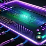
We often focus on the sleek exteriors and incredible user interfaces, but tucked away, out of sight, is the real unsung hero: the Printed Circuit Board, or PCB.
These little powerhouses are literally the brains and nervous system of every electronic gadget we love and rely on. From my own experience working in this space, I’ve seen firsthand how the traditional PCB design workflow has been completely reimagined.
It’s no longer just about meticulously placing components and drawing traces by hand; we’re talking about a dynamic, intricate dance of advanced materials, high-speed signal integrity, and incredibly clever software.
Think about the demand for miniaturization in our wearables, the lightning-fast requirements of 5G infrastructure, or the flexible circuits bending to fit innovative new product shapes.
It’s a challenging but hugely rewarding field, where precision and foresight are absolutely everything. And let me tell you, keeping up with these shifts—especially with AI now stepping in to automate and optimize like never before—is a full-time gig in itself!
The process of bringing a complex circuit board from a glimmer of an idea to a fully functional, manufacturable product is a journey filled with fascinating steps, careful considerations, and some truly ingenious problem-solving.
It’s a blend of art and science, requiring both deep technical expertise and a keen eye for detail. Trust me, understanding this process is key to appreciating the magic behind our modern world.
Let’s really get into the nitty-gritty of the PCB design workflow and uncover its secrets, starting right now!
The Spark of an Idea: From Concept to Schematic Capture

Honestly, it feels like magic sometimes, taking a vague notion for a new gadget and transforming it into something tangible. But before any physical board can even be considered, we have to start with the schematic.
This is where all the initial brainstorming gets translated into an electrical blueprint. I remember sitting down with designers, tossing around ideas for signal flow and power distribution, and then watching those ideas slowly coalesce into a detailed diagram.
It’s like mapping out the nervous system of your electronic brainchild, figuring out exactly how every component will talk to each other and what role each one plays.
This phase is absolutely critical because any fundamental errors here will ripple through the entire design process, costing way more time and money to fix down the line.
It’s a meticulous process, but when you nail it, you set the stage for something truly amazing.
Translating Vision into a Digital Blueprint
This isn’t just about drawing lines and symbols; it’s about translating a complex functional vision into a logical, electrical language. We’re talking about deciding on the microcontrollers, the memory chips, the power management ICs, and all the tiny resistors and capacitors that make everything tick.
Each connection represents a deliberate decision, ensuring that signals travel efficiently and power is supplied reliably. From my experience, the best designs come from a collaborative effort during this stage, where engineers, firmware developers, and even mechanical designers chime in.
Everyone brings their unique perspective, which helps catch potential issues early. It’s an iterative dance of refinement, ensuring that the digital blueprint accurately reflects the desired functionality and performance.
Why Component Selection Makes All the Difference
Choosing the right components isn’t just about finding something that “works.” It’s about optimizing for cost, performance, availability, and even long-term reliability.
I’ve seen projects grind to a halt because a critical component became obsolete or too expensive. It’s a constant balancing act. For instance, do you go for a cheaper, readily available op-amp, or invest in a higher-performance, lower-noise one that might be harder to source?
The decisions made here impact everything from the final product’s bill of materials (BOM) to its manufacturing yield. And let me tell you, keeping track of datasheets and supplier inventories is a full-time job in itself, especially with global supply chain fluctuations.
Getting this right from the start is paramount to avoiding headaches later on.
Laying Down the Digital Pathways: Mastering PCB Layout
Once the schematic is locked in, the real magic of bringing that blueprint to life begins with the PCB layout. This is where the abstract connections from the schematic transform into physical copper traces on a board.
From my hands-on perspective, this stage feels a lot like solving an incredibly intricate 3D puzzle under intense constraints. You’re not just placing components randomly; you’re meticulously arranging them to optimize for signal integrity, thermal management, manufacturability, and electromagnetic compatibility (EMC).
Every millimeter counts, especially with today’s miniature devices. I’ve spent countless hours zooming in and out, nudging components, and rerouting traces, trying to achieve that perfect balance.
It’s a creative process that blends engineering principles with a surprising amount of artistic intuition. Trust me, a well-laid-out board is a thing of beauty, performing flawlessly and looking elegant.
The Art of Component Placement
Proper component placement is probably one of the most underestimated aspects of PCB design. It’s not just about fitting everything onto the board; it’s about strategically positioning parts to minimize trace lengths, reduce noise, and ensure efficient thermal dissipation.
I always start by placing critical components like microcontrollers, power supplies, and high-speed connectors first, as their positions often dictate the layout of everything else.
Thinking about heat dissipation is also key – nobody wants a device that overheats! Often, grouping related components together can significantly simplify routing and improve overall performance.
It’s a constant battle between density, performance, and manufacturability, and honestly, every board presents its own unique challenges and opportunities.
Routing Traces: More Than Just Connecting Dots
This is where the copper pathways are drawn to connect all the components. But don’t let anyone tell you it’s just “connecting the dots.” High-speed signals require careful impedance control, differential pairs need precise matching, and power planes demand robust connections to minimize voltage drop.
I remember a project where seemingly minor routing errors led to intermittent signal loss that was incredibly difficult to diagnose. That experience really hammered home the importance of meticulous attention to detail here.
We’re talking about managing crosstalk, minimizing electromagnetic interference (EMI), and ensuring efficient current return paths. It’s a highly technical endeavor that requires a deep understanding of electrical principles and how they manifest in physical layouts.
Signal Integrity and Power Delivery: The Silent Guardians
These two often go unnoticed by the casual observer, but let me tell you, they are the absolute bedrock of a high-performing electronic device. Without solid signal integrity (SI) and robust power delivery, even the most innovative circuit will fall flat on its face.
From my own experience, diagnosing issues related to poor SI or PDN (Power Delivery Network) can be an absolute nightmare because the symptoms are often subtle and intermittent.
It’s like trying to find a ghost in the machine! This is where advanced simulation tools become indispensable, allowing us to predict and mitigate potential problems long before any physical board is fabricated.
Investing time in these areas upfront saves an incredible amount of grief and cost later on.
Taming High-Speed Signals
In today’s world of gigahertz processors and lightning-fast data transfers, ensuring signal integrity is more critical than ever. This means making sure that the electrical signals traveling along the traces don’t get distorted, reflected, or interfered with.
I’ve personally wrestled with issues like reflections caused by impedance mismatches, or crosstalk where signals jump from one trace to another. It’s not just about drawing a line; it’s about carefully considering trace width, spacing, layer stack-up, and termination strategies.
Every decision impacts how cleanly those high-speed bits arrive at their destination. This often involves intricate calculations and simulations to predict how signals will behave, especially in complex multi-layer boards.
Ensuring Robust Power for Flawless Performance
Just like our bodies need a steady supply of blood, electronic circuits demand a clean, stable power supply. A shaky power delivery network can lead to all sorts of issues, from erratic component behavior to complete system crashes.
Think of your computer suddenly glitching; often, it can be traced back to noise or dips in the power lines. My focus here is always on minimizing voltage drops, suppressing noise, and providing sufficient current to all components.
This often involves carefully designing power planes, adding decoupling capacitors near ICs, and ensuring low-inductance connections. It’s about creating a robust, quiet electrical environment where all your sensitive components can operate at their peak.
From Simulation to Reality: The Crucial Validation Steps
Before sending those meticulously crafted design files off to a manufacturer, there’s a vital phase of validation. This is where we put our design through its paces virtually, trying to catch any potential issues that might have slipped through.
Trust me, discovering a mistake after the boards are manufactured is a painful, expensive lesson. I’ve seen projects get delayed by weeks, sometimes months, because of overlooked details that could have been caught during simulation.
It’s an investment of time that pays dividends, ensuring that the first physical prototype has the best possible chance of working as intended. This stage also involves a deep dive into how the board will actually be built, which brings us to Design for Manufacturability.
Catching Gremlins Before Fabrication
This is where sophisticated software takes over to simulate everything from signal propagation to thermal performance. We’re looking for potential bottlenecks, excessive heat generation, or signals that might not arrive cleanly.
For instance, I’ll often run simulations to check for electromagnetic compatibility (EMC) issues, which can prevent a product from even passing certification.
It’s about digitally stress-testing the design, pushing it to its limits to see where it might break. Finding a layout error or a signal integrity problem in simulation is incredibly cheap to fix compared to spinning new prototypes.
This proactive approach saves not only money but also precious development time and reduces frustration for everyone involved.
Design for Manufacturability (DFM): The Fabricator’s Best Friend

Even a technically perfect design can be a nightmare to manufacture if DFM guidelines aren’t followed. This phase involves a rigorous review of the design against the specific capabilities and tolerances of the chosen PCB fabricator and assembler.
Are the trace widths and spaces within their limits? Are the drill sizes appropriate? Is there enough clearance between components for automated assembly?
I always try to put myself in the shoes of the manufacturing engineer. My goal is to make their job as easy as possible, which in turn leads to higher quality boards, fewer defects, and lower costs.
Over the years, I’ve learned that building strong relationships with manufacturers and understanding their processes makes a world of difference.
| Aspect | Key Consideration | Impact on Design |
|---|---|---|
| Material Selection | Dielectric constant, thermal properties, cost | Signal speed, heat dissipation, overall product cost |
| Layer Stack-up | Number of layers, impedance control, ground planes | Signal integrity, EMI reduction, board complexity |
| Component Footprints | Accuracy, IPC standards, manufacturability | Assembly yield, rework difficulty, electrical performance |
| Thermal Management | Via stitching, heatsinks, component placement | Component lifespan, device reliability, performance stability |
| Test Points | Accessibility, coverage, in-circuit test (ICT) | Ease of debugging, manufacturing test coverage, production cost |
The Human Element in Automation: Collaboration and Tools
It’s easy to get caught up in the sheer technicality of PCB design, but honestly, the human element—the collaboration, the shared knowledge, and the intuitive problem-solving—is just as crucial.
While software tools have become incredibly powerful, automating many mundane tasks, they’re ultimately extensions of our minds. I’ve found that the most successful projects are those where communication flows freely between everyone involved, from the electrical engineer dreaming up the schematic to the mechanical designer ensuring the board fits perfectly into its enclosure.
It’s a testament to how complex modern electronics are, requiring a blend of specialized expertise and seamless teamwork.
Beyond the Software: The Power of Teamwork
I’ve been on teams where everyone worked in silos, and let me tell you, it was a recipe for disaster. The best projects I’ve been a part of are those where we communicate constantly.
We’re talking about daily stand-ups, shared design reviews, and an open channel for questions and suggestions. For example, if the mechanical team decides to change the enclosure dimensions, that has immediate implications for my board layout.
Without quick communication, I might spend days optimizing a layout that’s no longer viable. It’s about building a shared understanding and working towards a common goal.
This kind of synergy dramatically reduces missteps and speeds up the entire development cycle, which is a huge win for everyone.
My Favorite Tools for Taming Complexity
While teamwork is vital, we can’t ignore the incredible power of modern PCB design software. Tools like Altium Designer, Eagle, and KiCad (for those who love open source!) have transformed the workflow.
I’ve personally spent thousands of hours in these environments, and the evolution of features, especially around simulation, routing automation, and design rule checking, has been phenomenal.
They allow us to manage immense complexity, from multi-layer boards with hundreds of components to high-speed designs with critical impedance requirements.
Finding a tool that fits your workflow and offers robust capabilities can really streamline your design process and boost your productivity. It’s an investment, but a truly worthwhile one if you’re serious about creating cutting-edge electronics.
Innovations on the Horizon: Where PCB Design is Headed
The world of PCB design is far from static; it’s constantly evolving, driven by the insatiable demand for smaller, faster, and more powerful electronics.
It’s an incredibly exciting time to be in this field because new technologies are emerging that are fundamentally changing how we approach board design.
From new materials that offer enhanced performance to the increasing integration of artificial intelligence, the future promises even more sophisticated and efficient ways to bring our electronic visions to life.
I’m always keeping an eye on these trends, as they often open up new possibilities and challenge us to think differently about what’s achievable.
AI and Machine Learning: Game Changers?
Artificial intelligence and machine learning are no longer just buzzwords; they’re beginning to make tangible impacts on the PCB design workflow. We’re seeing AI being used for automated routing, intelligent component placement optimization, and even predictive analysis for manufacturability issues.
I’ve played around with some of these new features, and while they’re still maturing, the potential is undeniable. Imagine a tool that learns from thousands of successful designs and can suggest optimal layouts or identify potential signal integrity issues before you even finish routing.
It’s not about replacing human designers but augmenting our capabilities, allowing us to tackle even more complex problems with greater speed and accuracy.
Embracing Flexible and Advanced Materials
Beyond the traditional rigid FR-4 boards, there’s a growing trend towards flexible PCBs (flex circuits) and even rigid-flex designs. These materials allow for incredibly innovative product form factors, fitting into spaces that were previously impossible.
Think about wearables that conform to the body or complex camera modules that bend around optical elements. On top of that, new high-performance materials are constantly being developed to meet the demands of higher frequencies and greater power densities.
These materials present new design challenges but also unlock incredible opportunities for miniaturization and enhanced performance. It’s a fascinating area, and I’m always eager to experiment with how these new materials can push the boundaries of what we can create.
Bringing It All Together: My Final Thoughts on This Wild Ride
Whew! We’ve covered a lot of ground today, from the initial spark of an idea in a schematic to the complex dance of PCB layout and the silent, yet critical, guardians of signal integrity and power delivery. Honestly, looking back at my own journey in electronics, it still astounds me how much meticulous detail and sheer brainpower goes into turning a conceptual sketch into a functioning piece of hardware. It’s a process that’s as much an art as it is a science, demanding patience, an insatiable curiosity, and a willingness to constantly learn and adapt. The satisfaction of seeing a design you’ve poured your heart into finally come to life, humming with purpose, is truly unmatched. It’s a testament to the fact that even in our increasingly digital world, there’s still incredible joy in building something tangible from the ground up.
I hope sharing these insights from my own experiences has given you a clearer picture of the intricate world of PCB design. It’s a field that can seem daunting at first, with countless acronyms and technical jargon, but trust me, with every successful design and every challenging debug session, you build a stronger foundation. Remember, every expert was once a beginner, and the most important thing is to keep experimenting, keep asking questions, and never stop pushing the boundaries of what you think is possible. The future of electronics is being designed right now, and who knows, maybe your next creation will be the one that changes the game!
Beyond the Bench: My Top 5 Pro Tips for Your Design Journey
1. Start Small, Learn Big: When you’re just getting your feet wet, resist the urge to jump into a super complex, multi-layer board with a high-speed processor. Begin with simpler projects – maybe a basic LED driver, a small microcontroller breakout board, or a sensor interface. Each successful small project builds confidence and reinforces fundamental concepts like power distribution, grounding, and component placement. I remember my first few designs felt like trying to solve a Rubik’s Cube blindfolded, but tackling manageable challenges step by step was the only way I truly learned to “see” the solutions. It’s all about iterative learning and celebrating those small victories.
2. Simulation is Your Best Friend, Not a Crutch: Seriously, embrace simulation tools early and often. Whether it’s SPICE for analog circuits, or more advanced signal integrity (SI) and power integrity (PI) tools for high-speed digital designs, they are invaluable. I’ve personally saved countless hours and dollars by catching potential issues in a virtual environment before ever sending a design to fabrication. Think of it as a virtual test bench where you can push your design to its limits without the risk of frying expensive components. It allows you to experiment freely, explore different scenarios, and understand the subtle behaviors of your circuits in a way that’s difficult to do with just a breadboard.
3. Build Relationships with Your Manufacturers: This might sound unconventional, but honestly, knowing your PCB fabricator and assembler is a game-changer. Don’t treat them just as anonymous vendors. Pick up the phone, ask questions about their capabilities, and understand their Design for Manufacturability (DFM) guidelines. I’ve found that a quick conversation about a tricky stack-up or a tight component placement can prevent costly errors and lead to much smoother production runs. They often have incredible insights from seeing thousands of different designs, and their advice can be golden. A good relationship fosters trust and ensures they’re invested in the success of your project too.
4. Document Everything, Seriously: I cannot stress this enough. From your initial design requirements and schematic revisions to layout choices and Bill of Materials (BOM) selections, document, document, document! Six months down the line, when you need to revise a board or hand it off to another engineer, a well-documented project is a lifesaver. I’ve been in situations where I had to reverse-engineer my *own* previous work because I got lazy with documentation, and trust me, that’s not a fun way to spend an afternoon. Clear comments in your schematic, detailed notes in your layout software, and version control for all your files will save you immense headaches in the long run.
5. Never Stop Learning and Adapting: The world of electronics, especially PCB design, is moving at lightning speed. New components are released daily, design tools gain new features constantly, and manufacturing processes evolve. What was best practice five years ago might be outdated today. Follow industry blogs, attend webinars, read datasheets (yes, all of them!), and engage with online communities. I personally set aside time each week just to read about new technologies and trends. Staying curious and continuously updating your knowledge isn’t just good practice; it’s essential for staying competitive and truly pushing the boundaries of what you can create. Embrace the learning journey, it’s an endless adventure!
The Nitty-Gritty: What Truly Sticks
At the core of everything we’ve discussed today, from initial concept to the thrill of a working prototype, lies a blend of methodical engineering and intuitive problem-solving. If there’s one thing I hope you take away, it’s that successful PCB design isn’t just about technical prowess; it’s about a holistic approach that values foresight, collaboration, and an unwavering attention to detail. The decisions made in the early schematic phase ripple through the entire process, underscoring the critical importance of a solid foundation.
Remember, validation and testing, both virtual and physical, are not optional steps but absolutely indispensable guardians against costly errors. And finally, never underestimate the power of human collaboration. Even with the most advanced automation tools at our fingertips, the shared expertise, diverse perspectives, and open communication within a team remain paramount for navigating the inherent complexities of modern electronic design. It’s a challenging, yet incredibly rewarding field, and I genuinely believe that with the right mindset and tools, anyone can contribute to shaping the future of technology, one meticulously crafted board at a time. Keep building, keep innovating, and let those creative circuits flow!
Frequently Asked Questions (FAQ) 📖
Q: What exactly is a PCB and why is its design process so critical in today’s electronic world?
A: You know, it’s funny how often we use devices without a second thought about what makes them tick. At its core, a Printed Circuit Board (PCB) is literally the foundation of almost every electronic device you can imagine – from your smartphone to your car’s navigation system, even your smart coffee maker!
It’s a flat board, usually made of an insulating material like fiberglass, with conductive pathways, or “traces,” etched onto its surface. These traces, typically copper, connect all the tiny electronic components like resistors, capacitors, and microchips, allowing them to communicate and work together.
Without a PCB, all those individual components would have to be connected by hand with a tangled mess of wires, making mass production impossible and devices clunky beyond belief.
The design process for a PCB is absolutely crucial because it directly impacts everything: a device’s performance, its reliability, how easy it is to manufacture, and ultimately, its cost.
Think about it like this: a well-designed PCB ensures that electrical signals flow seamlessly, minimizing issues like interference or power loss, which are huge for high-speed devices.
It’s also about making sure the device can withstand daily wear and tear, handle heat efficiently, and fit into those sleek, compact forms we’ve all come to expect.
From my experience, getting the design right early on saves a ton of headaches and money down the line. It’s truly the backbone, the central nervous system, that brings all the magic of modern electronics to life.
Q: What are the main steps involved in the modern PCB design workflow, especially with the push for advanced features and miniaturization?
A: The modern PCB design workflow is far more intricate and dynamic than it used to be, especially with everyone clamoring for smaller, faster, and more powerful gadgets.
From my perspective, having watched this industry evolve, it’s a detailed journey that begins long before any physical board is made. First, it all starts with schematic capture.
This is where engineers essentially draw a detailed blueprint of the circuit, outlining all the components and how they’re electrically connected. It’s like creating the architectural plans for a building.
Next, we move to component placement, which is a strategic game of Tetris. Here, designers meticulously arrange all those components on the board, considering everything from space optimization, thermal management (gotta keep those tiny parts cool!), and how signals will flow.
With miniaturization, this step is even more critical; we’re often talking about incredibly dense layouts where every micron counts. Then comes routing, which is literally drawing the copper traces that connect everything.
This isn’t just about making connections; it’s about ensuring signal integrity, minimizing electromagnetic interference (EMI), and maintaining proper impedance for high-speed signals.
With multi-layer boards becoming the norm, this becomes a complex, multi-dimensional puzzle. We also have to run rigorous design rule checks (DRC) throughout the process to catch any potential errors early, which believe me, saves a fortune compared to fixing them after manufacturing!
Finally, before anything goes to production, there’s a crucial Design for Manufacturability (DFM) review, ensuring the design isn’t just functional but also cost-effective and feasible for actual fabrication and assembly.
It’s a lot of back and forth, but that meticulousness is what yields the amazing devices we use every day.
Q: How is artificial intelligence (
A: I) transforming or enhancing the PCB design process? A3: Oh, AI in PCB design? It’s not just “enhancing” it; it’s genuinely revolutionizing how we approach things, and it’s something I’m personally incredibly excited about!
For years, PCB design involved a lot of repetitive, manual tasks and iterative trial-and-error, which was both time-consuming and, let’s be honest, prone to human mistakes.
Now, AI is stepping in as an incredibly powerful assistant. One of the biggest game-changers is automated component placement and routing optimization.
AI algorithms can analyze vast amounts of data and design constraints – think signal crosstalk, EMI, thermal dissipation, and minimizing trace lengths – to suggest optimal component placements and automatically route traces in ways that humans might miss or take days to figure out.
I’ve seen firsthand how this can drastically cut down on design cycles and even improve the performance of a board by finding more efficient layouts. Beyond just the initial layout, AI is also incredible for predictive analysis and simulation.
It can simulate electrical and thermal performance, helping designers identify potential issues like hotspots or signal integrity problems before a physical prototype is even built.
This means fewer costly re-spins and a faster time-to-market, which is gold in this competitive industry. It’s really about giving engineers superpowers, allowing us to focus on higher-level innovation and complex problem-solving rather than getting bogged down in the minutiae.
It’s truly a game-changer that’s making PCB design smarter, faster, and more precise.